

Free text
ReWio Short
Why atomic-scale precision decides whether billions of switches work
A modern microchip begins as something almost absurdly ordinary: sand. But by the time that material becomes the processor in a phone, a data center or a car, it has passed through one of the most demanding manufacturing systems ever created.
The central challenge is not simply making tiny parts. It is making billions of tiny electronic switches, then connecting them through a vast three-dimensional wiring system, layer after layer, with nearly no room for error. A defect too small to see with an ordinary microscope can ruin a chip. A layer shifted by a minute amount can disconnect a circuit. And every successful chip must perform reliably before it can leave the factory.
The journey starts with silicon, an element abundant in quartz-rich sand. For chipmaking, though, ordinary silicon is nowhere near clean enough. It must be refined to extraordinary purity, then formed into a single crystal. That crystal is shaped into a cylindrical ingot, sliced into thin discs, and polished until the surface is exceptionally flat and smooth. The result is a silicon wafer: usually a 300-millimeter disc, roughly 12 inches across and about as thin as a credit card.
One wafer is not one chip. It is the shared starting surface for many copies of a design. Depending on the size of the chip, a wafer can hold hundreds or thousands of individual dies. A die is the small piece of silicon that will eventually become a working processor, memory chip, sensor or other electronic device.
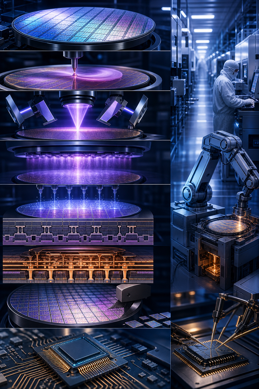
The wafer enters a fabrication plant, or fab. Inside, the air, temperature, humidity and vibration are controlled because microscopic contamination is a serious threat. A stray particle can be enormous compared with the smallest features being made. The fab is full of specialized tools, and wafers move through them in carefully managed sequences for weeks. The same basic operations repeat again and again: grow or deposit a film, coat it, expose a pattern, develop it, etch it, clean it, measure it, and repeat.
First comes the task of placing materials on the wafer. Some layers are grown directly from silicon, such as silicon dioxide, an insulating material made by exposing silicon to oxygen or steam at high temperature. Other layers are deposited by delivering gases or other precursor materials into a chamber, where a film forms on the wafer. These films can be insulators, semiconductors, metals or barriers that keep materials from reacting or diffusing where they should not.
Deposition is not just about putting material down. Thickness, composition and uniformity matter across the whole wafer. In some cases, atomic layer deposition builds a film through controlled chemical reactions that add material in extraordinarily thin increments. After material is added or removed, the wafer may also be polished through chemical-mechanical planarization. That combines chemistry with gentle abrasion to restore a flat surface. Flatness matters because the next layer must be printed in focus across the wafer.
Then comes the process most people associate with chipmaking: lithography. Think of it as transferring a blueprint to the wafer with light, but at a scale where the analogy quickly becomes inadequate.
A machine coats the wafer with photoresist, a light-sensitive chemical film. The wafer is baked, then loaded into a lithography system. A patterned mask, often called a reticle, contains one layer of the chip’s design. The system projects a reduced image of that pattern onto selected regions of the wafer. The exposure changes the photoresist chemically. During development, some parts of the resist dissolve away, leaving a patterned protective stencil.
For many layers, manufacturers use deep-ultraviolet light. For the most intricate layers of leading-edge chips, they can use extreme ultraviolet, or EUV, lithography. EUV light has a wavelength of 13.5 nanometers, far shorter than the 193-nanometer light used in advanced deep-ultraviolet systems. Shorter wavelengths help print smaller features.
Creating and steering EUV light is a remarkable engineering problem in itself. In ASML’s laser-produced plasma source, tiny molten tin droplets are fired through the system at high speed. Laser pulses first flatten a droplet, then vaporize it into a plasma that emits EUV light. This happens tens of thousands of times per second. EUV is absorbed by most materials, so the optical path operates in a high vacuum. And instead of familiar glass lenses, EUV systems use exquisitely precise multilayer mirrors to guide and focus the light.
The exposed photoresist pattern does not become the chip by itself. It tells the next process where action is allowed. In etching, the wafer is exposed to chemicals or plasma. Material that is not protected by the hardened resist is selectively removed. The remaining structure may form part of a transistor, an insulating boundary, a contact opening or a path for future wiring. Then the resist is stripped away, and the wafer is cleaned for the next operation.
Another essential step is doping. Pure silicon is a semiconductor: its ability to conduct electricity can be controlled. To create useful electronic devices, manufacturers introduce extremely small, controlled amounts of other elements into selected regions. One common method is ion implantation, which sends a beam of charged atoms into exposed regions of the wafer. A later heating step helps repair crystal damage and activate the dopants.
Doping creates regions with different electrical behavior. Combined with precisely formed insulating and conductive structures, those regions make transistors. A transistor is a switch: an electrical signal can control whether current flows. Logic chips combine immense numbers of these switches into circuits that store bits, make calculations, move data and coordinate everything from graphics to artificial intelligence.
But a sea of transistors is not yet a useful processor. They have to be connected. This is the back end of wafer fabrication, where manufacturers build a stack of interconnect layers above the transistors. Dielectric materials keep wires electrically separated. Metal layers, commonly based on copper in modern interconnect schemes, form the horizontal wiring. Tiny vertical connections, called vias, link one metal layer to the next.
This wiring stack is why a chip is truly three-dimensional. A signal may travel from a transistor, up through a vertical connection, across one metal level, down through another, and onward through many more paths. Power must reach the circuitry. Signals must arrive on time. Resistance, capacitance, heat and electromagnetic interference all have to be managed. As transistors shrink, wiring can become as limiting as the transistors themselves.
Now consider alignment. A leading-edge chip may contain scores of patterned layers. Each new pattern must be placed in the correct relationship to structures already buried beneath it. This is called overlay. If the placement is wrong, even by a very small amount, a contact may miss its target, a wire may narrow too much, or a transistor may behave unpredictably.
The problem is not static. Wafers can bend slightly. Materials expand and contract with temperature. Earlier processing can alter the wafer’s shape. Optical components warm during use. The lithography system must therefore locate alignment marks, compensate for variation and place each exposure accurately across the wafer. Metrology and inspection tools continually measure thickness, feature size, focus, defects and layer-to-layer alignment. Their results feed back into the process, allowing engineers and automated control systems to correct drift before it becomes widespread waste.
That feedback loop explains why chipmaking is more than a sequence of machines. It is a manufacturing conversation between chemistry, optics, mechanics, software, measurement and statistics. A process that works perfectly on a test wafer is not enough. It must produce a high proportion of good dies, repeatedly, at production scale. That proportion is yield, and yield is one of the hardest measures to improve.
When fabrication is complete, the wafer holds a grid of finished dies. Before it is cut apart, automated test equipment can probe electrical contacts on each die while it is still on the wafer. This wafer sort identifies dies that meet the required electrical behavior and flags ones that do not.
The wafer is then diced into individual dies. A good die still is not ready to be installed in a computer. Its microscopic contacts need protection, power delivery, heat removal and durable connections to a circuit board. That is the job of packaging.
In a conventional package, a die is mounted on a substrate and connected through tiny bumps or other interconnects. The package provides external contacts and often helps move heat toward a heat spreader or cooling system. Increasingly, advanced packaging can place several dies side by side or stack them, connecting them at very short distances. That allows designers to combine compute, memory and other specialized chiplets into one package.
Testing continues throughout assembly. Manufacturers may test separated dies, test the finished package, subject parts to elevated temperatures or electrical stress, and run system-level tests that look for subtle faults under more realistic conditions. Chips can also be sorted, or binned, according to the performance and power characteristics they actually achieve.
So the finished microchip is not merely a tiny object. It is the final result of thousands of tightly controlled operations, repeated across an ultra-pure wafer and verified at every stage. Its billions of transistors work only because materials were placed, patterned, etched, doped, polished, aligned, wired, packaged and tested with astonishing discipline.
The memorable fact is this: the miracle of a microchip is not that engineers can make something small. It is that they can make an entire hidden city of switches and wires, layer by layer, and persuade almost all of it to work together.